|
The semiconductor industry is in the era of 32nm process, and it is expected that it will meet 16nm around 2019. Designing a 45nm SoC costs USD20-50 million except labor cost, and the design of a 32nm SoC costs USD75-120 million, while it is less than USD5 million for 130nm. Therefore, even if the IC design companies with annual revenue of over USD2 billion probably can not afford such high cost, and there are no more than ten such companies all over the world, which means that the majority of IC design companies are disqualified to enter 45nm or 32nm era. Perhaps the semiconductor industry will develop at the pace of Moore’s Law. Having made up for the bottleneck of process shrinkage, the packaging industry will yield unusually brilliant results in post-Moore’s Law era.
In practice, the packaging industry has become increasingly important since 2000, and the debut of BGA, FC and CSP has sped up the progression of semiconductor industry. However, the front-end of semiconductor manufacturing has been in stagnancy, still in the era of 12-inch wafer, and it is likely that 15-inch wafer era will not come. Currently, a revolutionary packaging, TSV packaging presents itself, which is so called 3D IC. The technology will dramatically improve chip transistor density, cubic density rather than plane density, and make semiconductor industry surpass the development pace of Moore’s Law. Not only packaging companies and wafer OEMs, but also nearly all global prominent semiconductor companies such as IBM, Samsung, Intel and Qualcomm are all actively developing TSV technology. TSV has been in large shipment in image sensor and MEMS field, and it will rapidly expand to memory field in the future, and to DSP, RF IC, cell phone baseband, processor, CPU and GPU in 2013. Furthermore, TSV market size will rise to over US$2 billion from less than US$ 300 million currently, which will be the rapidest growing field in semiconductor industry.
In the meantime, the advanced packaging has an increasingly powerful driving force. IC advanced packaging mainly refers to IC substrate packaging, including BGA, CSP, FC and LGA, and it mainly applies for cell phone, memory, PC (CPU, GPU and Chipest), network communications, and consumer electronics. In addition, the network communications include high-speed switch, router and base station. Consumer electronics are as the followings such as game console, IPOD, ITOUCH, and high-end PMP. The cell phone has more and more powerful functions, thinner and thinner in size; and the smart phones have covered a rising ratio. In the field of memory, DDR3 has become the mainstream, with the rate increased to over 1GHz; CPU has multi-cores, and the number of pins has exceeded 1,200. China’s 3G and the world’s 4G network distribution has boosted up the sales of base stations. The stay-at-home economy has made game machine shipment increase sharply as well.
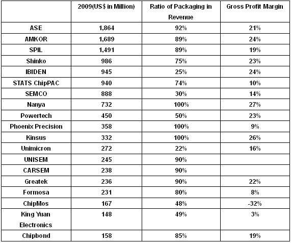
Revenue Forecast of Global 19 IC Advanced Packaging Manufacturers, 2009

Japan and Taiwan have almost dominated IC packaging industry. Among the global top 12 companies, seven of which are from Taiwan, two from Japan, two from the United States, and one from South Korea.
For more details, please visit http://www.researchinchina.com/Htmls/Report/2009/5772.html |