Next-generation Zonal Communication Network Topology and Chip Industry Research Report, 2024
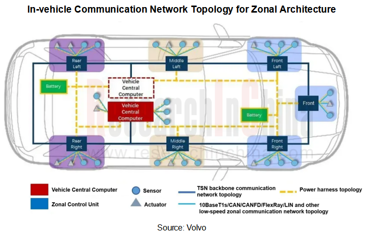
The in-vehicle communication architecture plays a connecting role in automotive E/E architecture. With the evolution of automotive E/E architecture, in-vehicle communication technology is also developing continuously. The core of communication technology development is the communication interface protocol. In the in-vehicle communication framework based on next-generation Zonal architecture:
BUS communication: It mainly includes automotive Ethernet (10M/100M/1000M/2.5G/5G/10G, etc.), CAN-XL, CAN-FD, etc. The underlying layer of CAN-XL/CAN-FD BUS communication is the transceiver chip, and automotive Ethernet chip includes PHY chip and switch chip. Under the Zonal architecture, automotive backbone network will use automotive Ethernet, and local low-speed networks will continue to use CAN-FD/LIN in a short term. After the 10Base-T1S automotive Ethernet and CAN-XL products are scaled up, they may become the main application of low-speed networks in Zonal architecture.
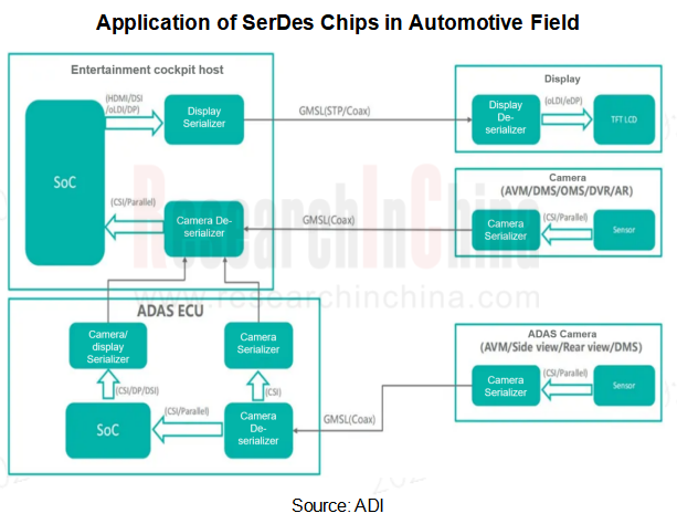
High-speed video streaming communication: Currently, there are multiple protocols for vehicle SerDes chips, mainly including FPD-Link, GMSL, MIPI A-PHY, ASA-ML, etc. Automotive high-speed video streaming transmission uses serial transmission technology, which requires a SerDes to implement. Major application scenarios include video transmission from camera to ADAS SoC and content transmission from cockpit SoC to vehicle display.
Short-range wireless communication: Mainly includes Bluetooth, WIFI, NFC, UWB and NearLink, and main application scenarios include phone-car connectivity, digital car key, wireless BMS, etc.
Inter-chip communication: Mainly includes PCIe, NVLink and other protocols. Under the central supercomputing + Zonal architecture, there are many cascading applications between multiple SoC chips. PCIe is mainly used for communication between CPU and GPU, and NVLink is mainly used for communication between GPUs.
High-speed video streaming communication: How can in-vehicle SerDes chips help OEMs reduce costs and increase efficiency?
Vehicle SerDes chip is mainly used for real-time data transmission of image and video signals from in-vehicle camera to ADAS domain controller, cockpit domain controller, vehicle display, etc. It is usually composed of two chips: Serializer and De-serializer. A complete set of communication protocols must be available between serializer and de-serializer to achieve complete, secure and accurate data transmission.
Necessity of 10G+ vehicle SerDes communication: The development of 10G+ vehicle SerDes chips is closely related to development trends of automotive central integration + Zonal architecture, end-to-end autonomous driving, in-vehicle through-type integrated display screen and ultra HD image quality.
HD camera: In deep learning models, high-resolution image data is required for target recognition. In order to be able to identify and monitor targets at greater distances, some manufacturers have launched automotive cameras with more than 8MP. For example, Sony Semiconductor released the 17MP automotive image sensor IMX735 in 2023; Sunny Optical also announced the completion of R&D of a 17MP front-view automotive lens. At present, an 8MP camera generates up to 5.76Gbps of data per second. In the future, to achieve data transmission of higher-definition cameras, the bandwidth requirement must reach 10Gbps or more.
High-resolution display: The bandwidth requirements for information exchange between intelligent cockpit domain and in-vehicle display are also increasing. Taking Geely Galaxy E8 as an example, the bandwidth requirement for its 45-inch 8K through-type integrated screen can reach 12.7Gbps.
Necessity of in-vehicle SerDes chip integration solution: In the foundation model era, if a camera can achieve 320° full-view coverage, the number of cameras required will double. Vehicle SerDes chips are used in pairs. If a single camera is equipped with a pair of serializer/de-serializers, the demand for vehicle SerDes chips in the vehicle will surge. The additional cables, plug-ins and other related connectors will not only be detrimental to vehicle lightweight, but will also increase its manufacturing cost, which is contrary to the overall development trend of the vehicle and cost reduction needs of OEMs. For vehicles using the next-generation Zonal architecture and AI foundation model, the integrated solution of serializers and de-serializers is particularly important, which helps to simplify circuit design, reduce the use of SerDes chips and wiring harnesses and connectors.
Automotive SerDes protocols can be mainly divided into private protocols and public protocols, and current global automotive SerDes market is dominated by the former. ADI's GMSL and TI's FPD-Link almost monopolize the global automotive SerDes market share. In order to break the industry monopoly, more and more automotive SerDes chip vendors have emerged in China, such as Rsemi, Kungao Micro, Motorcomm, etc.
?
Since TI and ADI have already occupied the first-mover advantage and absolute monopoly in the low-speed automotive SerDes products (1.6Gbps~6Gbps), Chinese manufacturers have planned high-speed automotive SerDes products (above 10Gbps) to meet the high-bandwidth needs of future intelligent vehicles in order to seize the first-mover advantage in mass production of high-speed automotive SerDes products.
?
Take Rsemi's self-developed single-channel 16Gbps automotive high-performance SerDes chip R-LinC as an example. It is backward compatible with the full rate of 16Gbps-1.6Gbps, uses a private protocol, and supports long-distance transmission of 15 meters. Built with a 22nm process, the insertion loss compensation capability reaches more than 30dB, and can achieve real-time adaptive equalization. R-LinC is mainly used for long-distance real-time transmission from sensors such as automotive cameras to SoCs. Its single-channel 16Gbps rate can meet extreme needs of current ultra-high-resolution cameras (such as 17MP) for image data transmission.
?
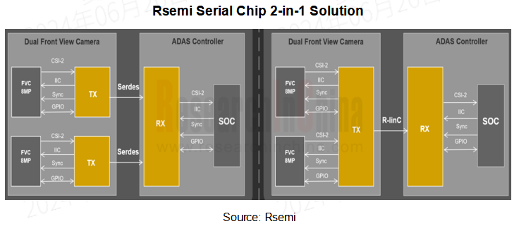
For sensor side, with the support of 16Gbps high-speed transmission, one Rsemi R-LinC serial chip can connect to two 8MP high-definition cameras simultaneously, and a single wiring harness can transmit two video streams, saving one chip and one set of wiring harnesses and connectors, helping to efficiently reduce costs for current mainstream visual sensor solutions.
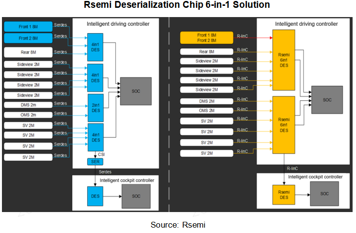
On the controller side, a single Rsemi R-LinC deserializer can realize 6-way input and a high-speed data throughput of up to 6*16Gbps (12 8MP cameras), while supporting a forwarding capability of 16Gbps. Therefore, 1-2 de-serializers can cover the mainstream intelligent driving vision solutions in the current market. Combined with new 6-in-1 connector, the board-level hardware design area is smaller, the device layout is better, and the system solution cost is greatly reduced.
Currently, average number of cameras configured in visual sensors of intelligent vehicles has exceeded 5. High-end intelligent driving requires 11 cameras to complete the coverage of entire vehicle's surrounding environment. For this reason, Rsemi has joined hands with Sony Semiconductor to launch the "Intelligent Driving 5V Super Vision Solution".
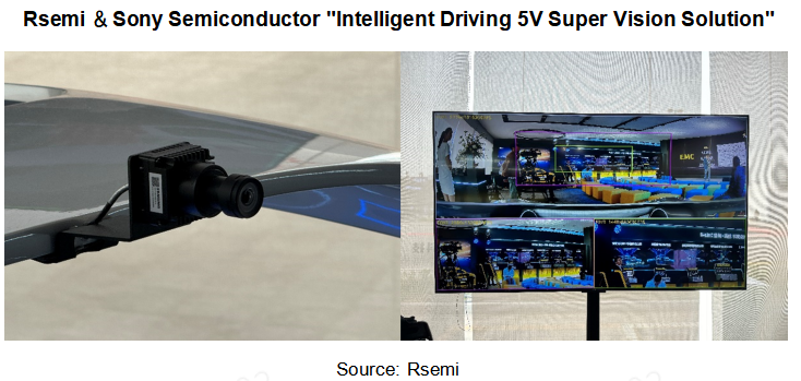
Hardware configuration: The solution consists of 1 front-view ultra-high-definition camera based on Sony's 17M image sensor (IMX735) + 4 super fisheye cameras based on Sony's 8MP + 5 Rsemi 16Gbps high-speed serial chips (RLC91603) + 1 highly integrated 6-in-1 deserialization chip (RLC99602);
5 cameras cover entire vehicle's intelligent driving full FOV: In this solution, the front-view 17MP camera can output three images from wide angle to narrow angle simultaneously, which can replace the existing two mainstream front-view 8MP cameras; the other four 8MP-12MP ultra-wide-angle fisheye cameras can also also serve as around-view camera to complete the panoramic coverage of entire vehicle;
Advantages of R-LinC serializer/de-serializer in 5V solution: In terms of sensors, one RSemi R-LinC serialization chip can meet the transmission rate of Sony's 17MP ultra-high-definition camera, saving one serialization chip and one set of wiring harnesses and connectors, thus significantly reducing costs. In terms of controllers, the solution only requires one RSemi R-LinC de-serializer to achieve 5-way video stream input, and with the highly integrated new connector, it helps to reduce the board-level hardware design area, optimize device layout, and reduce system solution costs.
There are currently three public standards for automotive SerDes: MIPI A-PHY, ASA-ML, and HSMT.
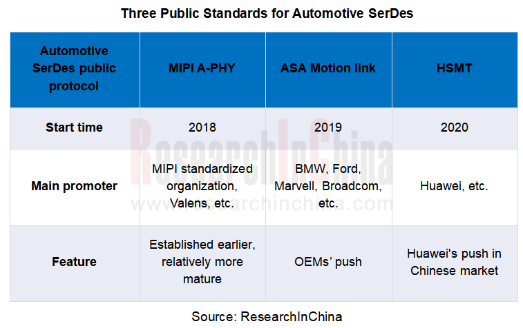
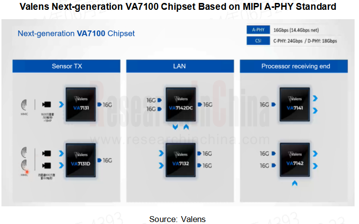
Valens is an important contributor to the MIPI A-PHY standard and the first vendor on the market to provide chipsets (VA7000 series) that comply with A-PHY standard, targeting ultra-high-speed network applications in ADAS and autonomous drive subsystems. In the planning route of Valens A-PHY chips, it is expected to launch a more powerful VA7100 chipset in 2025. A single interface can support bandwidths of more than 16Gbps, resolutions of up to 17MP, and can access camera and radar data simultaneously. At the processing receiving end, a single link can support bandwidths of more than 16Gbps, enabling the transmission or exchange of multiple channels of real-time video and data, and all sensor data can be flexibly exchanged and copied.
The ASA Motion Link (ASA-ML) specification is mainly promoted by BMW, Ford, Marvell, and Broadcom. In March 2024, BMW Group announced at the Automotive Ethernet Conference in Munich that it would introduce standardized ASA-ML in 2027. In addition, BMW and Microchip also cooperated to conduct a chipset concept verification based on the ASA-ML standard. In the future, BMW is very likely to use Microchip's VS77X chipset for high-speed video image transmission between sensors and domain controllers & displays.
The HSMT standard is mainly promoted by Chinese companies such as Huawei.
However, public protocols nowadays such as A-PHY, ASA-ML, and HSMT have not been finally frozen and are still being updated. They have not passed the verification of large-scale product shipments, nor have they been widely accepted and adopted by the industry. There are still many uncertainties.
Since SerDes is a bridge chip across components, it is used in pairs in actual applications, and interoperability is not a rigid requirement. Relatively speaking, private protocols are more efficient, simple and mature, so the development path of SerDes standardization remains to be seen.
How to build the next-generation in-vehicle communication architecture under the Zonal architecture?
In next-generation Zonal architecture, after realizing functional centralization, the number of ECUs in the car will be greatly reduced. Functional centralization is mainly guided by software algorithms, but to be truly implemented, it must rely on physical hardware such as controller, SoC, communication chip, and power chip in zonal controller and central computing platform to support it.
Communication requirements of cross-domain integration + Zonal architecture for in-vehicle backbone network
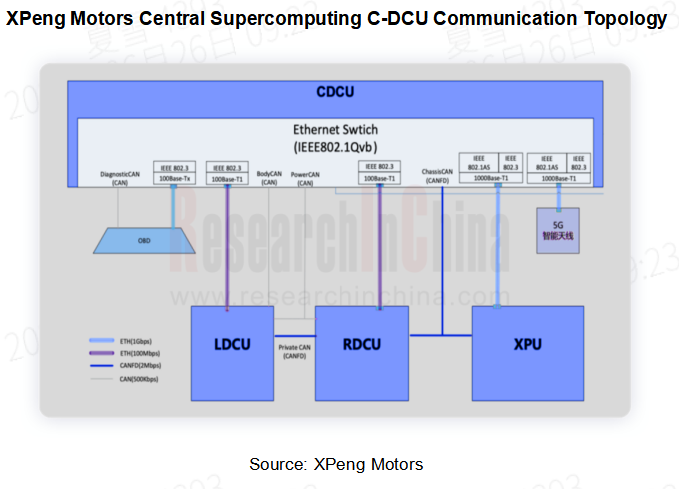
XPeng Motors X-EEA3.0: The central supercomputer C-DCU integrates cockpit, partial vehicle body, central gateway and other functions. In the communication of this central supercomputer, C-DCU contains one Automotive Ethernet switch to support TSN, which is connected to XPU and 5G smart antenna through 2 channels of Gigabit Ethernet 1000Base-T1. It also contains 6 channels of 100M Ethernet, 2 of which are connected to the left and right Zonal controllers (LDCU, RDCU). MCUs of central computing platform and two zonal controllers are all Renesas' third-generation 28nm high-speed MCUs.
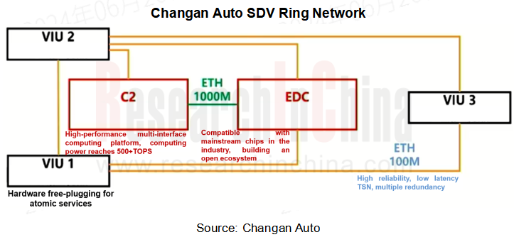
Changan Auto SDV ring network: Changan Auto's SDV ring network: Changan Auto SDA architecture consists of C2 (central computer: computing power 508TOPS) + EDC (experience data computer: computing power 2000GFLOPS) + three zonal controllers VIU. The architecture adopts vehicle Ethernet ring network communication technology, with 100M Ethernet as the backbone network. C2 and EDC communicate through Gigabit Ethernet. At the same time, TSN, ring network redundancy and other technologies are applied to solve the problems of disordered data transmission and packet loss in traditional Ethernet.
Communication requirements of next-generation central computing + Zonal architecture for in-vehicle backbone network
In the next-generation central computing + Zonal architecture, Zonal controller will generally integrate Zonal gateways, high-speed communication MCUs, vehicle Ethernet switch chips, Ethernet PHY chips and other communication-related chip devices. Each Zonal gateway contains an Ethernet switch, and a car may need 6-7 chips.
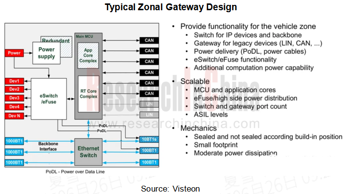
Some typical solutions under Zonal architecture:
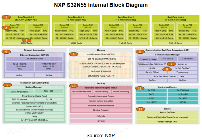
High-speed communication MCU (NXP): In March 2024, NXP launched the world's first 5nm automotive MCU, the S32N55, which integrates vehicle dynamic control, body, comfort, and central gateway, and has multiple network interfaces, including CAN, LIN, FlexRay, automotive Ethernet, CAN-FD, CAN-XL, and PCIe, with at least 15 CAN network interfaces.
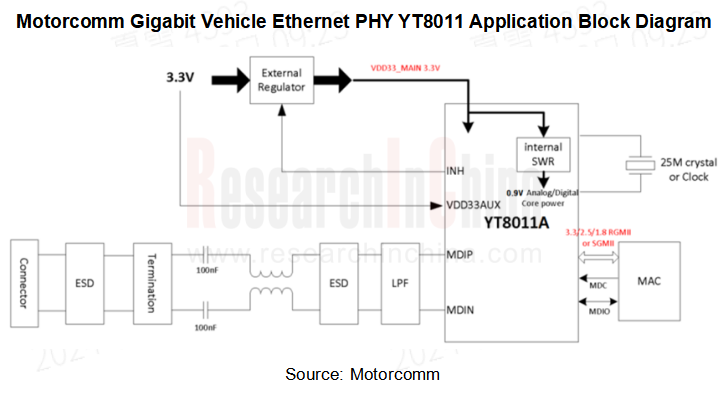
Automotive Ethernet PHY chip (Motorcomm): By the end of 2023, Motorcomm's first Gigabit automotive Ethernet PHY chip product YT8011 was successfully mass-produced and obtained orders from multiple OEMs. The YT8011 series chips are compatible with 100BASE-T1 and 1000BASE-T1, support RGMII/SGMII MAC interface, support EEE energy-saving Ethernet, 1588 time synchronization protocol, IEEE802.1AS time synchronization protocol, and can achieve a transmission distance of more than 60 meters on unshielded twisted pair cables, fully meeting the application requirements of high-speed data transmission such as radar, surround view, and autonomous driving.
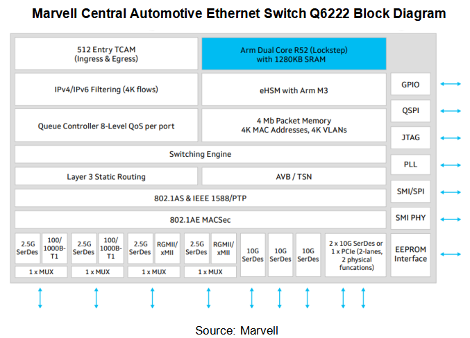
Automotive Ethernet switch chip (Marvell): Marvell's central automotive Ethernet switch series Brightlane Q622x includes two products, Q6222 and Q6223, which are specially designed for automotive Zonal architecture. Among them, Q6223 has a bandwidth of 90 Gbps, which is almost twice the capacity of currently available automotive switches; Q6222 contains nine 60 Gbps ports, including five 10G SerDes ports, four 2.5G SerDes ports and two 1000Base-T1 PHYs to choose from. This zonal switch aggregates the traffic from devices in physical area of ??the car and connects to central computing switch through high-speed Ethernet to achieve information interaction.
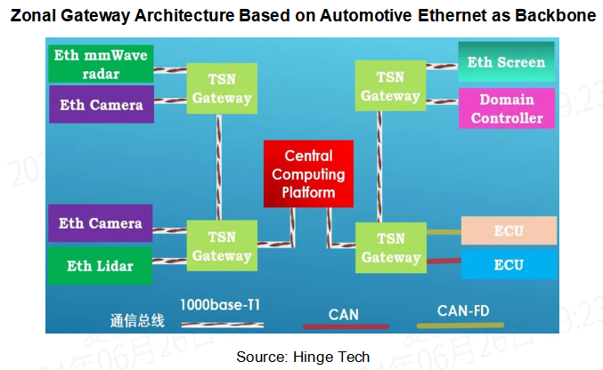
Hinge Tech has designed a zonal gateway architecture based on automotive Ethernet as the backbone network: after the sensor collects data, it is transmitted to corresponding TSN zonal gateway through automotive Ethernet for data exchange. Zonal gateway then transmits corresponding data to the central computing platform via automotive Ethernet bus for calculation and processing. After central computing platform calculates and processes the data, it is transmitted to the domain controller through TSN gateway for decision or automotive Ethernet display (Eth Screen) for display. Meanwhile, TSN zonal gateway is compatible with CAN/CAN-FD communication, and exchanges information with corresponding CAN ECU through the CAN bus and CAN-FD bus.
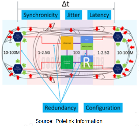
In the future, considering the demand for data transmission in autonomous driving and requirements for functional safety in the vehicle, the large amount of data transmission migration between central and zonal controllers, and the interaction of software algorithms, 10G+ automotive Ethernet may become the data backbone link in Zonal architecture.
Inter-chip interconnection becomes the key to communication in HPC central computing platform
Central computing platform is the core part of Zonal architecture. Since all systems that require a certain scale of computing resources, such as intelligent driving, intelligent cockpit, and vehicle control, will be concentrated in a central computing unit, multiple processors or SoCs will be used, which puts high demands on the computing power, interface, data security, functional safety and many other aspects of central computing platform's hardware architecture. The central computing platform is a heterogeneous chip integrated design of CPU+GPU, and communication technologies such as inter-board interconnection, inter-chip interconnection, and on-chip interconnection are key. Therefore, under Zonal architecture, automotive network also faces an important challenge, which is the high-performance computing interconnection of central computing platform itself.
In heterogeneous computing architecture, GPU and CPU are usually connected together through PCIe bus to work together. Currently, there are two major automotive-grade PCIe switch manufacturers on the market, one is Microchip, which focuses on mid-to-high-end products, and the other is PERICOM, which was acquired by Renesas and focuses on the low-end market and does not support NTB.
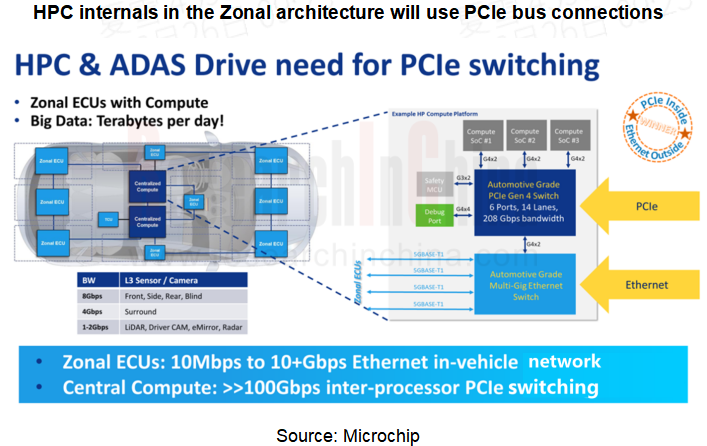
During foundation model training, the full potential of high-end graphics card clusters depends on whether each GPU in the GPU server cluster can communicate quickly and smoothly. In a multi-GPU system, the bandwidth of inter-GPU communication is usually above hundreds of GB/s. Data transmission rate of PCIe bus can easily become a bottleneck, and the serial-to-parallel conversion of PCIe link interface will produce a large delay, affecting efficiency and performance of GPU parallel computing.
Thus, NVIDIA launched NVLink technology that can improve communication between GPUs. NVLink is used in SoCs, and the in-vehicle computing platform NVIDIA DRIVE Thor integrates many intelligent functions such as digital dashboard panel, in-vehicle infotainment, autonomous driving, parking, etc. into a single architecture. In March 2024, NVIDIA launched the fifth-generation NVLink, with a total bandwidth of up to 1.8 TB/s, which is more than14 times that of PCIe 5.0. A single NVLink Switch chip has 50 billion transistors and supports seamless high-speed communication between up to 576 GPUs, which is suitable for complex large language models.
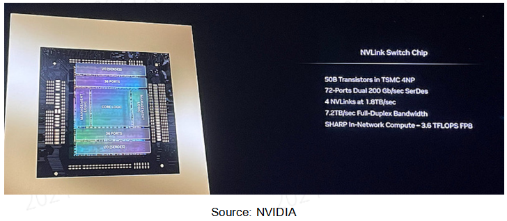
NVIDIA Blackwell architecture is based on the fifth-generation NVLink technology and is designed for Transformer, Large Language Model (LLM) and generative AI workloads. It can be divided into B200 and GB200 product series. The GB200 GPU integrates one Grace CPU and two B200 GPUs. Compared with the H100 Tensor Core GPU with NVLink 4, the GB200 NVL72 can provide 30 times the performance improvement for Large Language Model (LLM) inference loads, and reduce the cost and energy consumption of building and running real-time generative AI large language models on trillions of parameters to one-twenty-fifth of the previous level.
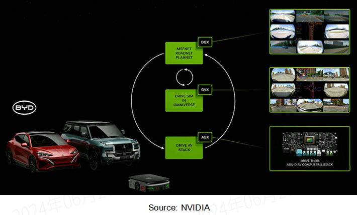
In March 2024, NVIDIA announced an expansion of its cooperation with BYD. BYD's future electric vehicles will be equipped with NVIDIA's next-generation autonomous vehicle processor DRIVE Thor using the Blackwell architecture. DRIVE Thor is expected to start mass production as early as 2025, with a performance of up to 1000 TFLOPS. In addition, BYD will also use NVIDIA's AI infrastructure for autonomous driving model training, and smart factory robots will also use the NVIDIA Isaac robot system.